|
|
||||||||||||||||||||||||||||||||
 |
Introduction | |||||||||||||||||||||||||||||||
|
Verilog has built in primitives like gates, transmission gates, and switches. These are rarely used in design (RTL Coding), but are used in post synthesis world for modeling the ASIC/FPGA cells; these cells are then used Verilog HDL 已经构建了诸如门(gates)、传输门和开关电路等基本原语。这些原语很少使用在RTL级编码设计中,但是却使用在ASIC/FPGA单元的建模的后期综合中。这些单元使用门级仿真或者称之为SDF simulation. 用于布局、布线工具(P & R tool)的由综合工具产生的网表格式使用的也是Verilog HDL的门级原语。 |
||||||||||||||||||||||||||||||||
|
|
||||||||||||||||||||||||||||||||
|
Note : RTL engineers still may use gate level primitivies or ASIC library cells in RTL when using IO CELLS, Cross domain synch cells. 注意: RTL级的工程师仍然使用门级原语,或者使用IO 单元,跨域的同步单元的的RTL级的ASIC二进制单元 |
||||||||||||||||||||||||||||||||
|
|
||||||||||||||||||||||||||||||||
|
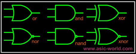
Gate Primitives //门级原语 N-input( N 输入) | |||||||||||||||||||||||||||||||
|
|
||||||||||||||||||||||||||||||||
 |
||||||||||||||||||||||||||||||||
|
|
||||||||||||||||||||||||||||||||
|
The gates have one scalar output and multiple scalar inputs. The 1st terminal in the list of gate terminals is an output and the other terminals are inputs. 这些门都是有一个标量输出,多个标量输入。门的端表中的第一个端是输出,其他端都是输入(译者注,这里说的是门级原语的参数表的分布方式,)。 |
||||||||||||||||||||||||||||||||
|
|
||||||||||||||||||||||||||||||||
|
||||||||||||||||||||||||||||||||
|
|
||||||||||||||||||||||||||||||||
 |
Examples //举例 |
|||||||||||||||||||||||||||||||
  1 module gates();
  2
  3 wire out0;
  4 wire out1;
  5 wire out2;
  6 reg  in1,in2,in3,in4;
  7
  8 not U1(out0,in1);
  9 and U2(out1,in1,in2,in3,in4);
 10 xor U3(out2,in1,in2,in3);
 11
 12 initial begin
 13   $monitor(
 14   "in1=%b in2=%b in3=%b in4=%b out0=%b out1=%b out2=%b",
 15    in1,in2,in3,in4,out0,out1,out2);
 16   in1 = 0;
 17   in2 = 0;
 18   in3 = 0;
 19   in4 = 0;
 20    #1  in1 = 1;
 21    #1  in2 = 1;
 22    #1  in3 = 1;
 23    #1  in4 = 1;
 24    #1  $finish;
 25 end
 26
 27 endmodule
You could download file gates.v here |
||||||||||||||||||||||||||||||||
|
|
||||||||||||||||||||||||||||||||
 in1 = 0 in2 = 0 in3 = 0 in4 = 0 out0 = 1 out1 = 0 out2 = 0
 in1 = 1 in2 = 0 in3 = 0 in4 = 0 out0 = 0 out1 = 0 out2 = 1
 in1 = 1 in2 = 1 in3 = 0 in4 = 0 out0 = 0 out1 = 0 out2 = 0
 in1 = 1 in2 = 1 in3 = 1 in4 = 0 out0 = 0 out1 = 0 out2 = 1
 in1 = 1 in2 = 1 in3 = 1 in4 = 1 out0 = 0 out1 = 1 out2 = 1
|
||||||||||||||||||||||||||||||||
|
|
||||||||||||||||||||||||||||||||
|
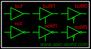
Transmission Gate Primitives //传输门原语 N-output(N输出) | |||||||||||||||||||||||||||||||
|
Transmission gates are bi-directional and can be resistive or non-resistive. 传输门是双向的,并且分为阻抗型和非阻抗型。 |
||||||||||||||||||||||||||||||||
|
|
||||||||||||||||||||||||||||||||
|
Syntax: keyword unique_name (inout1, inout2, control); //语法格式 |
||||||||||||||||||||||||||||||||
|
|
||||||||||||||||||||||||||||||||
 |
||||||||||||||||||||||||||||||||
|
|
||||||||||||||||||||||||||||||||
|
||||||||||||||||||||||||||||||||
|
|
||||||||||||||||||||||||||||||||
|
Transmission gates tran and rtran are permanently on and do not have a control line. Tran can be used to interface two wires with seperate drives, and rtran can be used to weaken signals. 传输门中tran 和 rtran 因为没有control line(控制线),所以是永久有效(on)。 Tran主要用来面向有着两个驱动的双线, rtran主要用于削弱信号。 |
||||||||||||||||||||||||||||||||
|
|
||||||||||||||||||||||||||||||||
|
Examples //举例 | |||||||||||||||||||||||||||||||
|
|
||||||||||||||||||||||||||||||||
  1 module transmission_gates();
  2
  3 reg data_enable_low, in;
  4 wire data_bus, out1, out2;
  5
  6 bufif0 U1(data_bus,in, data_enable_low);
  7 buf  U2(out1,in);
  8 not U3(out2,in);
  9
 10 initial begin
 11   $monitor(
 12     "@%g in=%b data_enable_low=%b out1=%b out2= b data_bus=%b",
 13     $time, in, data_enable_low, out1, out2, data_bus);
 14   data_enable_low = 0;
 15   in = 0;
 16    #4  data_enable_low = 1;
 17    #8  $finish;
 18 end
 19
 20 always  #2  in = ~in;
 21
 22 endmodule
You could download file transmission_gates.v here |
||||||||||||||||||||||||||||||||
|
|
||||||||||||||||||||||||||||||||
 @0 in = 0 data_enable_low = 0 out1 = 0 out2 = 1 data_bus = 0
 @2 in = 1 data_enable_low = 0 out1 = 1 out2 = 0 data_bus = 1
 @4 in = 0 data_enable_low = 1 out1 = 0 out2 = 1 data_bus = z
 @6 in = 1 data_enable_low = 1 out1 = 1 out2 = 0 data_bus = z
 @8 in = 0 data_enable_low = 1 out1 = 0 out2 = 1 data_bus = z
 @10 in = 1 data_enable_low = 1 out1 = 1 out2 = 0 data_bus = z
|
||||||||||||||||||||||||||||||||
|
|
||||||||||||||||||||||||||||||||
|
|
||||||||||||||||||||||||||||||||
|
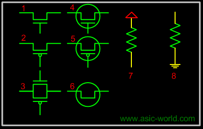
Switch Primitives //开关电路语言 | |||||||||||||||||||||||||||||||
|
There are six different switch primitives (transistor models) used in Verilog, nmos, pmos and cmos and the corresponding three resistive versions rnmos, rpmos and rcmos. The cmos type of switches have two gates and so 在Verilog中有6个不同的开关原语 (晶体管模型): nmos, pmos, cmos,和对应的三种有阻抗的 (resistive)rnmos, rpmos, rcmos. cmos类型的开关电路有两个门组成,因此也有两个控制信号。 |
||||||||||||||||||||||||||||||||
|
|
||||||||||||||||||||||||||||||||
|
Syntax: keyword unique_name (drain. source, gate) //开关原语的语法 (漏极、源极、栅极) |
||||||||||||||||||||||||||||||||
|
|
||||||||||||||||||||||||||||||||
 |
||||||||||||||||||||||||||||||||
|
|
||||||||||||||||||||||||||||||||
|
||||||||||||||||||||||||||||||||
|
|
||||||||||||||||||||||||||||||||
|
Transmission gates are bi-directional and can be resistive or non-resistive. Resistive devices reduce the signal strength which appears on the output by one level. All the switches only pass signals from source to drain, 传输门是双向的可以有阻抗也可以无阻抗。带阻抗的设备在下一级输出时,降低信号强度。所有的开关电路都只能将信号从source 传向 drain,(即从源极到漏极)。不正确的设备布线,将导致高阻输出(Z)。 |
||||||||||||||||||||||||||||||||
|
|
||||||||||||||||||||||||||||||||
|
Examples //举例 switch name(drain,source ,gate) | |||||||||||||||||||||||||||||||
|
|
||||||||||||||||||||||||||||||||
 1 module switch_primitives();
 2
 3 wire  net1, net2, net3;
 4 wire  net4, net5, net6;
 5
 6 tranif0 my_gate1 (net1, net2, net3);
 7 rtranif1 my_gate2 (net4, net5, net6);
 8
 9 endmodule
You could download file switch_primitives.v here |
||||||||||||||||||||||||||||||||
|
|
||||||||||||||||||||||||||||||||
|
Transmission gates tran and rtran are permanently on and do not have a control line. Tran can be used to interface two wires with separate drives, and rtran can be used to weaken signals. Resistive devices reduce the 传输门tran和tran由于没有控制线,可以永久有效。Tran能够驱动具有分别驱动的双线。rtran能够用来削弱信号。阻抗设备的下一级输出将削弱信号。 所有的开关只将信号从source传送到drain,设备间不正确的连线,将导致高阻输出。 |
||||||||||||||||||||||||||||||||
|
|
||||||||||||||||||||||||||||||||
|
Logic Values and signal Strengths // 逻辑值和信号强度 | |||||||||||||||||||||||||||||||
|
The Verilog HDL has got four logic values // Verilog HDL有4个逻辑值: 0, 1, X(未知), Z(高阻)。 |
||||||||||||||||||||||||||||||||
|
|
||||||||||||||||||||||||||||||||
|
||||||||||||||||||||||||||||||||
|
|
||||||||||||||||||||||||||||||||
|
Verilog Strength Levels //Verilog中 强度级别 | |||||||||||||||||||||||||||||||
|
|
||||||||||||||||||||||||||||||||
|
