High-gain, high-bandwidth… how can I get it all?
Achieving high gain (1000-V/V or more) and high bandwidth (tens of MHz) simultaneously can be a challenge as we are forced to use multiple
stages. Besides the circuit requirements of high gain and high bandwidth, the critical issues to pay close attention to are noise and stability.
Check out the below diagram to see the overall architecture in a 3-stage amplifier.
The noise contribution of each successive amplifier will add as an RMS sum with the earlier stages weighted by the gain of the later stages.
For a 3-stage architecture, this can be expressed as:
Whereas the gain will simply be multiplied together, as shown below.
So far we have circuit architecture and a couple of equations, but very little detail on its implementation. With the noise equation, the
first stage is going to be the limiting factor.
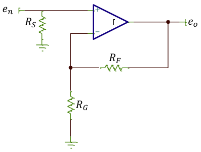
The non-inverting input stage noise, shown below in Figure 1, in a high-gain configuration can be modeled as:
Figure 1: simplified noise model
We now know that we need to pick an amplifier with the lowest possible voltage noise. Since we want to achieve as high a gain as possible
in the first stage, while maintaining good bandwidth, we will look at the lowest voltage noise amplifier possible with the highest Gain Bandwidth Product (GBWP). Take a quick look at the parametric search yields below.
|
Part Number |
Input Voltage Noise Density (nV/rtHz) |
GBWP (MHz) |
|
0.85 |
3900 |
|
|
1.1 |
1800 |
|
|
0.69 |
3900 |
Let’s select the LMH6629 for
the first stage since we want to develop a +5-V system. Looking at a gain of 50-V/V, we will then achieve 78MHz.
Of course, we could select the same LMH6629 for
any of the other stages, but since the input voltage noise specs do not have to be as good as that of the first stage, we extend the search to encompass any device to achieve high-bandwidth and high-gain. Current feedback amplifiers and maintaining the bandwidth
almost independently of the gain will be the best choice here. Check out the below table to see a breakdown.
|
Part Number |
Gain @ BW (V/V) |
BW (MHz) |
Comment |
|
100 |
35 |
Lowest power solution |
|
|
100 |
70 |
Highest equivalent GBWP |
|
|
16 |
350 |
Highest BW solution |
Here we can consider either inverting or non-inverting gain circuits depending on the amplifier and the desired bandwidth. TheOPA695 will
achieve lower noise in an inverting configuration whereas the OPA683 and OPA684 will
achieve lower noise in the non-inverting configuration.
Since we are set to achieve high gain on a single stage (100-V/V), the gain resistor can be as low as 10 W. In an inverting topology, this
may set an additional constraint on the driving stage. The gain resistor should be maintained between 10 W and 50 W, while the feedback resistor should not exceed 1.5k W. Remember that the frequency response will be limited by the feedback resistor (RF),
and the feedback capacitor (CF) pole resulting in a parasitic feedback capacitor due to the component, layout, etc…
Putting all this together and replacing the ideal amplifiers from figure 1 above yields figure 2 below.
Figure 2: Implementation of a 100,000-V/V multi-stage amplifier with 10MHz bandwidth.
RC filters were inserted between the stages to minimize the noise contribution. The overall frequency response and -3dB bandwidth can be
approximated to 6 first-order pole [1].
Stay tuned for part two, where we will look at the stability issues associated with this circuit.


