Abstract
DE2 CD所提供的Reference Design無疑是最佳的Nios II範本,他將DE2所有的周邊都驅動了,不過對於初學者來說,一些高級的周邊(如TV Decoder、Audio CODEC等...)暫時用不到,還增加了複雜度,DE2_NIOS_Lite僅留下最常用的周邊與IP,方便初學者學習與debug。
Introduction
使用環境:Quartus II 7.2 SP3 + Nios II EDS 7.2 SP3 + ModelSim-Altera 6.1g + DE2(Cyclone II EP2C35F627C6)
會想整理出DE2_NIOS_Lite,主要有幾個原因
1.DE2太強大,但對初學者而言,常用的周邊大概就只有CLOCK、KEY、SW、LEDG、LEDR、7SEG、onchip memory、SRAM、SDRAM與Flash而已,在top module與SOPC Builder多了這麼多暫時用不到的Verilog與IP,只會讓Nios II的學習曲線更為陡峭,並增加debug的複雜度。
2.DE2的reference design無法在ModelSim-Altera仿真,在(原創) 如何使用ModelSim-Altera對Nios II仿真? (SOC) (Nios II) (SOPC Builder) (ModelSim) (DE2)為了能仿真,只用了onchip memory,並對gcc做最佳化設定,但這並非長遠之計,而DE2_NIOS_Lite使用了主流的SDRAM,並在ModelSim-Altera仿真成功。
DE2_NIOS_Lite.v / Verilog
2 (C) OOMusou 2008 http://oomusou.cnblogs.com
3
4 Filename : DE2_NIOS_Lite.v
5 Compiler : Quartus II 7.2 SP3 + ModelSim-Altera 6.1g
6 Description : DE2_NIOS lite version
7 Release : 08/08/2008 1.0
8 */
9
10 module DE2_NIOS_Lite (
11 input CLOCK_50, // On Board 50 MHz
12 input [3:0] KEY, // Pushbutton[3:0]
13 input [17:0] SW, // Toggle Switch[17:0]
14 output [8:0] LEDG, // LED Green[8:0]
15 output [17:0] LEDR, // LED Red[17:0]
16 output [6:0] HEX0, // Seven Segment Digit 0
17 output [6:0] HEX1, // Seven Segment Digit 1
18 output [6:0] HEX2, // Seven Segment Digit 2
19 output [6:0] HEX3, // Seven Segment Digit 3
20 output [6:0] HEX4, // Seven Segment Digit 4
21 output [6:0] HEX5, // Seven Segment Digit 5
22 output [6:0] HEX6, // Seven Segment Digit 6
23 output [6:0] HEX7, // Seven Segment Digit 7
24 inout [15:0] DRAM_DQ, // SDRAM Data bus 16 Bits
25 output [11:0] DRAM_ADDR, // SDRAM Address bus 12 Bits
26 output DRAM_LDQM, // SDRAM Low-byte Data Mask
27 output DRAM_UDQM, // SDRAM High-byte Data Mask
28 output DRAM_WE_N, // SDRAM Write Enable
29 output DRAM_CAS_N, // SDRAM Column Address Strobe
30 output DRAM_RAS_N, // SDRAM Row Address Strobe
31 output DRAM_CS_N, // SDRAM Chip Select
32 output DRAM_BA_0, // SDRAM Bank Address 0
33 output DRAM_BA_1, // SDRAM Bank Address 0
34 output DRAM_CLK, // SDRAM Clock
35 output DRAM_CKE, // SDRAM Clock Enable
36 inout [7:0] FL_DQ, // FLASH Data bus 8 Bits
37 output [21:0] FL_ADDR, // FLASH Address bus 22 Bits
38 output FL_WE_N, // FLASH Write Enable
39 output FL_RST_N, // FLASH Reset
40 output FL_OE_N, // FLASH Output Enable
41 output FL_CE_N, // FLASH Chip Enable
42 inout [15:0] SRAM_DQ, // SRAM Data bus 16 Bits
43 output [17:0] SRAM_ADDR, // SRAM Address bus 18 Bits
44 output SRAM_UB_N, // SRAM Low-byte Data Mask
45 output SRAM_LB_N, // SRAM High-byte Data Mask
46 output SRAM_WE_N, // SRAM Write Enable
47 output SRAM_CE_N, // SRAM Chip Enable
48 output SRAM_OE_N // SRAM Output Enable
49 );
50
51 wire CPU_CLK;
52 wire CPU_RESET;
53
54 assign FL_RST_N = 1'b1;
55
56 Reset_Delay u0 (
57 .iRST(KEY[0]),
58 .iCLK(CLOCK_50),
59 .oRESET(CPU_RESET)
60 );
61
62 SDRAM_PLL u1 (
63 .inclk0(CLOCK_50),
64 .c0(DRAM_CLK),
65 .c1(CPU_CLK)
66 );
67
68 nios_ii u2 (
69 .clk(CPU_CLK),
70 .clk_50(CLOCK_50),
71 .reset_n(CPU_RESET),
72 // KEY
73 .in_port_to_the_key_pio(KEY),
74 // SW
75 .in_port_to_the_sw_pio(SW),
76 // LEDG
77 .out_port_from_the_ledg_pio(LEDG),
78 // LEDR
79 .out_port_from_the_ledr_pio(LEDR),
80 // SEG7
81 .oSEG0_from_the_seg7(HEX0),
82 .oSEG1_from_the_seg7(HEX1),
83 .oSEG2_from_the_seg7(HEX2),
84 .oSEG3_from_the_seg7(HEX3),
85 .oSEG4_from_the_seg7(HEX4),
86 .oSEG5_from_the_seg7(HEX5),
87 .oSEG6_from_the_seg7(HEX6),
88 .oSEG7_from_the_seg7(HEX7),
89 // SDRAM
90 .zs_addr_from_the_sdram(DRAM_ADDR),
91 .zs_ba_from_the_sdram({DRAM_BA_1,DRAM_BA_0}),
92 .zs_cas_n_from_the_sdram(DRAM_CAS_N),
93 .zs_cke_from_the_sdram(DRAM_CKE),
94 .zs_cs_n_from_the_sdram(DRAM_CS_N),
95 .zs_dq_to_and_from_the_sdram(DRAM_DQ),
96 .zs_dqm_from_the_sdram({DRAM_UDQM,DRAM_LDQM}),
97 .zs_ras_n_from_the_sdram(DRAM_RAS_N),
98 .zs_we_n_from_the_sdram(DRAM_WE_N),
99 // SRAM
100 .SRAM_ADDR_from_the_sram(SRAM_ADDR),
101 .SRAM_CE_N_from_the_sram(SRAM_CE_N),
102 .SRAM_DQ_to_and_from_the_sram(SRAM_DQ),
103 .SRAM_LB_N_from_the_sram(SRAM_LB_N),
104 .SRAM_OE_N_from_the_sram(SRAM_OE_N),
105 .SRAM_UB_N_from_the_sram(SRAM_UB_N),
106 .SRAM_WE_N_from_the_sram(SRAM_WE_N),
107 // FLASH
108 .address_to_the_cfi_flash(FL_ADDR),
109 .data_to_and_from_the_cfi_flash(FL_DQ),
110 .read_n_to_the_cfi_flash(FL_OE_N),
111 .select_n_to_the_cfi_flash(FL_CE_N),
112 .write_n_to_the_cfi_flash(FL_WE_N)
113 );
114
115 endmodule
top module相當精簡,唯一比較特殊的就是delay與產生SDRAM所要的clock。
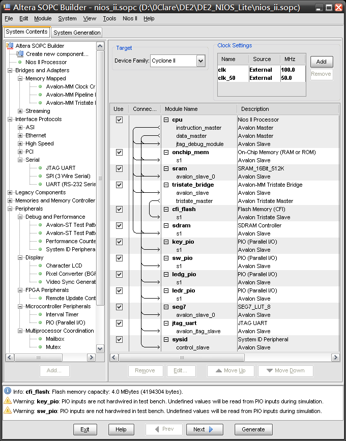
SOPC Builder僅含最常用的IP。
完整程式碼下載
DE2_NIOS_Lite.7z
Conclusion
學習Nios II有兩個門檻,一個是top module的Verilog,一個是SOPC Builder的設定,只要稍微沒弄好,就是『Leaving target processor paused』的錯誤訊息,希望藉由這個簡化過的版本,減少初學者學習Nios II的挫折感。
See Also
(原創) 如何自己用SOPC Builder建立一個能在DE2上跑μC/OS-II的Nios II系統? (IC Design) (DE2) (Quartus II) (Nios II) (SOPC Builder) (μC/OS-II)
(原創) 如何使用ModelSim-Altera對Nios II仿真? (SOC) (Nios II) (SOPC Builder) (ModelSim) (DE2)
(原創) 如何解決Nios II的『Leaving target processor paused』的錯誤訊息? (IC Design) (Quartus II) (SOPC Builder) (Nios II)
(原創) DE2_NIOS_Lite 1.1 (SOC) (Nios II) (SOPC Builder) (μC/OS-II) (DE2)
(原創) 如何自己用SOPC Builder建立一個能在DE2上跑μC/OS-II的Nios II系統 (SRAM精簡版)? (SOC) (Quartus II) (Nios II) (SOPC Builder) (μC/OS-II) (DE2)
(原創) DE2_NIOS_Lite 1.2 (SOC) (Nios II) (SOPC Builder) (DE2)